MYD-C7Z015 Development Board
MYD-C7Z015 Development Board
The MYD-C7Z015 development board is a programmable, low-cost and high-performance board designed by MYIR. It integrates Xilinx XC7Z015 (Z-7015) Dual-core ARM Cortex-A9 Processor with Xilinx 7-series FPGA logic from Xilinx Zynq-7000 family, with one PCIe interface and one SFP transceiver module interface on the base board to allow users to expand numerous of high-speed devices. It’s typically applications ranges from Industrial Automation, Test & measurement, Medical Equipment, Aerospace to military and more others.
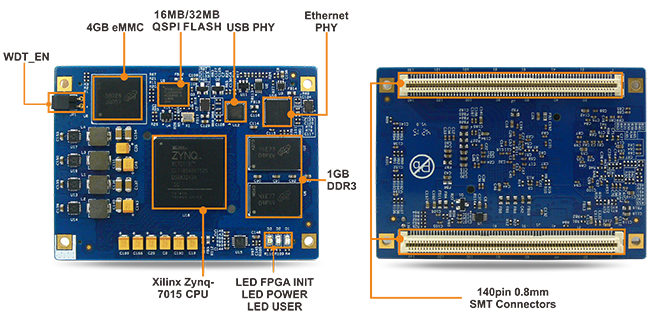
MYC-C7Z015 CPU Module
- MYC-C7Z015 CPU Module as Controller Board
- Two 0.8mm pitch 140-pin Connectors for Board-to-Board Connections
- 766MHz Xilinx XC7Z015 Dual-core ARM Cortex-A9 Processor with Xilinx 7-series FPGA logic
- 1GB DDR3 SDRAM, 4GB eMMC, 32MB QSPI Flash
- Serial port, 4 x USB Host, Gigabit Ethernet, CAN, HDMI, LCD, TF
- 1 x XADC, 3 x PMoD, 1 x FMC, 1 x SFP Module, 1 x PCIe
- Optional 4.3 or 7 inch LCD/TSP
- Ready-to-Run Linux 5.4.0
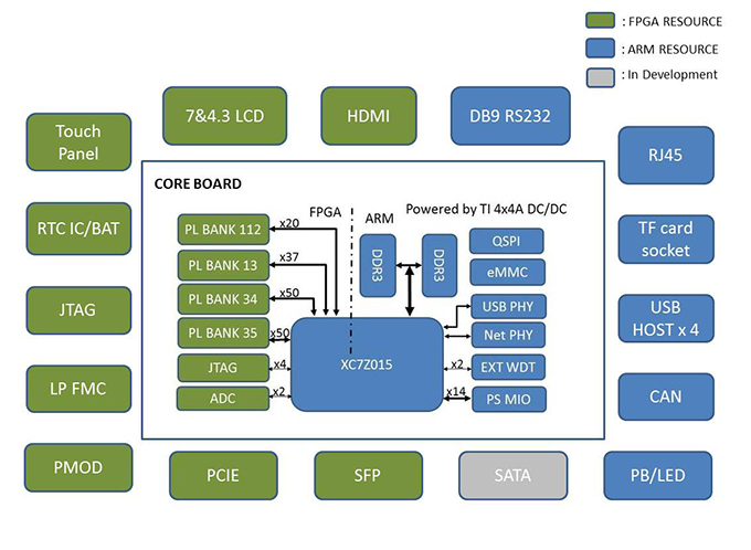
The MYD-C7Z015 development board is using the MYC-C7Z015 CPU Module as the core controller board which integrates the core components including the Zynq-7015 processor, 1GB DDR3 SDRAM, 4GB eMMC, 32MB quad SPI Flash, a Gigabit Ethernet PHY, a USB PHY and external watchdog. The MYC-C7Z015 CPU Module is mounted on to the MYD-C7Z015 base board through two 0.8mm pitch 140-pin Board-to-Board connectors. Compared with the Zynq-7010, the processor Zynq-7015, has more logic cells, Block RAM and DSP slices, which makes the board obtain more powerful programmable function for users.
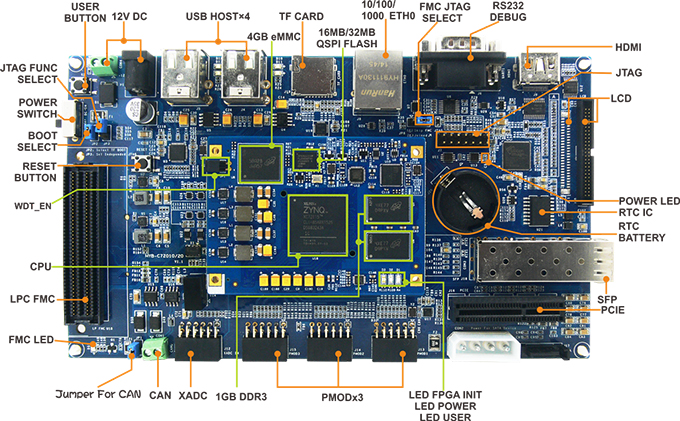
MYD-C7Z015 Development Board
The MYD-C7Z015 development board takes full features of the Zynq-7015 SoC to create a rich set of peripherals to the base board through headers and connectors including one RS232 serial port, four USB Host ports, one Gigabit Ethernet port, CAN, HDMI, LCD/Touch screen, TF card slot, RTC, one XADC header to allow you take advantage of Xilinx XADC and one low-pin count FMC connector to allow various FMC cards for custom I/O options. Especially, it has one SFP transceiver module to keep higher transmission speed and better stability during your evaluation, as well as one PCIe interface, which contributes the data transmission speed to a high frequency when customers using the board.
Features
Mechanical Parameters
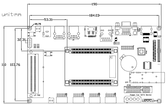
- Dimensions: 190mm x 110mm (base board), 75mm x 55mm (CPU Module)
- PCB layers: 4-layer design (base board), 12-layer design (CPU Module)
- Power supply: 12V/0.5A (base board), 5V/0.5A (CPU Module)
- Working temp.: -40~85 Celsius (industrial grade)
SoC
- Xilinx XC7Z015-2CLG485 (Zynq-7015)
- 766MHz ARM® dual-core Cortex™-A9 MPCore processor (up to 866MHz)
- Integrated Artix-7 class FPGA subsystem with 74K logic cells, 46,200 LUTs, 160 DSP slices
- NEON™ & Single / Double Precision Floating Point for each processor
- Supports a Variety of Static and Dynamic Memory Interfaces
- Four high-speed SerDes transceivers up to 6.25Gbps
- Four PCIe Gen2 hardened, integrated IP blocks
Memory
- 1GB DDR3 (2 x 512MB, 32-bit)
- 4GB eMMC
- 32MB QSPI Flash (16MB is optional)
Peripherals and Signals Routed to Pins
- 10/100/1000M Ethernet PHY
- One USB PHY
- External watchdog
- Three LEDs
- One blue LED for power indicator
- One red LED for FPGA program done indicator
- One green user LED
- Two 0.8mm pitch 140-pin board-to-board expansion connectors bring out below signals:
- One Gigabit Ethernet
- One USB OTG 2.0
- Up to two Serial ports
- Up to two I2C
- Up to two CAN BUS
- *Serial ports, I2C and CAN signals will be reused in PS part, or implemented through PL pins
- One SPI (can be implemented through PL pins)
- ADC (one independent differential ADC, 16-channel ADC brought out through PL pins)
- One SDIO
- Bank 13 (PL I/O configurable as up to 18 LVDS pairs and 1 single-ended I/O or 37 single-ended I/O)
- Bank 34 (PL I/O configurable as up to 24 LVDS pairs and 2 single-ended I/O or 50 single-ended I/O)
- Bank 35 (PL I/O configurable as up to 24 LVDS pairs and 2 single-ended I/O or 50 single-ended I/O)
- Bank 112 (4 GTP serial transceivers, 2 reference clock input)
OS Support
- Linux 5.4.0
The MYD-C7Z015 Base Board (MYB-C7Z015)
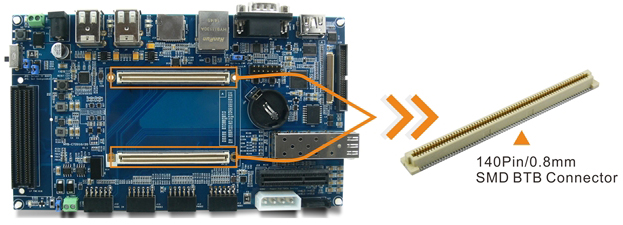
MYD-C7Z015 Base Board (MYB-C7Z015)
PS Unit
- Four USB 2.0 Host ports (through USB Hub)
- One RS232 (DB9 port)
- One TF card slot (bootable)
- One CAN interface
- One 10/100/1000M Ethernet
- One 2.54mm pitch 14-pin JTAG interface (PS, PL reused)
- Battery backed RTC
- One User Button (One I2C, can be connected to LCD and Resistive Touch Screen)
- Jumpers
- One for booting selection from TF card or QSPI
- One for JTAG selection for using PS and PL reused or independent JTAG configured through PL pins
- One for selection if adding FMC module to JTAG
PL Unit
- One XADC interface
- One Xilinx standard LPFMC interface
- One HDMI interface (16-bit YCrCb, support 1080p display, do not support audio)
- LCD/Touch screen interface (16-bit RGB, signals reused with HDMI, supports resistive and capacitive touch screen)
- Two LEDs (one for FMC module detection, one for power indicator)
- Three-channel PMoD
- One SFP transceiver module with RJ45 interface (SFP-GE-T module, up to 1000Mbps)
- One PCIe interface
Order Part No and Packing List
| Item | Part No. | Included |
|---|---|---|
|
MYD-C7Z015 |
MYD-C7Z015-4E1D-766-I |
- One MYD-C7Z015 Board |
|
MYC-C7Z015-4E1D-766-I |
- One MYC-C7Z015 CPU Module |
Hardware Specification
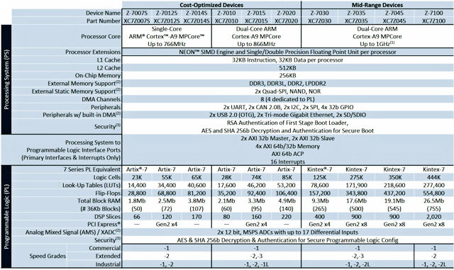
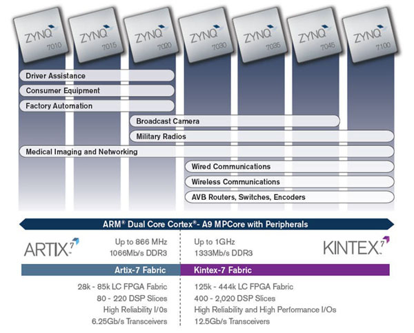
The Zynq™-7000 family of devices combines the software programmability of a Processor with the hardware programmability of an FPGA, resulting in unrivaled levels of system performance, flexibility, scalability while providing system benefits in terms of power reduction, lower cost with fast time to market. Unlike traditional SoC processing solutions, the flexible programmable logic of the Zynq-7000 devices enables optimization and differentiation, allowing designers to add peripherals and accelerators to adapt to a broad base of applications.
The Zynq-7000 AP SoC leverages the 28nm scalable optimized programmable logic used in Xilinx’s 7 series FPGAs. Each device is designed to meet unique requirements across many use cases and applications. The Z-7010, Z-7015, and Z-7020 leverage theArtix®-7 FPGA programmable logic and offer lower power and lower cost for high-volume applications. The Z-7030, Z-7035, Z-7045, and Z-7100 are based on the Kintex®-7 FPGA programmable logic for higher-end applications that require higher performance and high I/O throughput.
Software Features
The MYD-C7Z015 development board is preloaded with Linux 5.4.0. MYIR provides software package in product disk along with the goods delivery. The software package features as below:
| Item | Features | Description | Remark |
|---|---|---|---|
| Cross compiler | gcc 9.2.0 | arm-xilinx-linux-gnueabi-gcc (GCC) 9.2.0 | |
| Boot program | BOOT.BIN | First boot program including FSBL, bitstream | Source code provided |
| u-boot | Secondary boot program | Source code provided | |
| Linux Kernel | Linux 5.4.0 | Customized kernel for MYC-C7Z015 | Source code provided |
| Drivers | USB Host | USB Host driver | Source code provided |
| PCI-E | PCIE driver | Source code provided | |
| SFP | SFP transceiver driver | Source code provided | |
| Ethernet | Gigabit Ethernet driver | Source code provided | |
| MMC/SD/TF | MMC/SD/TF card driver | Source code provided | |
| CAN | CAN driver | Source code provided | |
| LCD Controller | XYLON LCD driver | Source code provided | |
| HDMI | HDMI (SII902X chip) driver | Source code provided | |
| Button | Button driver | Source code provided | |
| UART | Serial port driver | Source code provided | |
| LED | LED driver | Source code provided | |
| GPIO | GPIO driver | Source code provided | |
| QSPI | QSPI Flash S25FL256S driver | Source code provided | |
| RTC | DS3231 RTC driver | Source code provided | |
| Resistive Touch | TSC2007 resistive touch screen driver | Source code provided | |
| Capacitive Touch | FT5X0X capacitive touch screen driver | Source code provided | |
| ADC | ADC driver | Source code provided | |
| File System | Ramdisk | Ramdisk system image | |
| RootFS | Build from buildroot tools, With Qt 5.11.3 | ||
| Ubuntu Desktop 18.04 | tar archive file and SD image |
| İşlemci Tipi | : | Xilinx |


