MYD-J7A100T Development Board
MYD-J7A100T Development Board
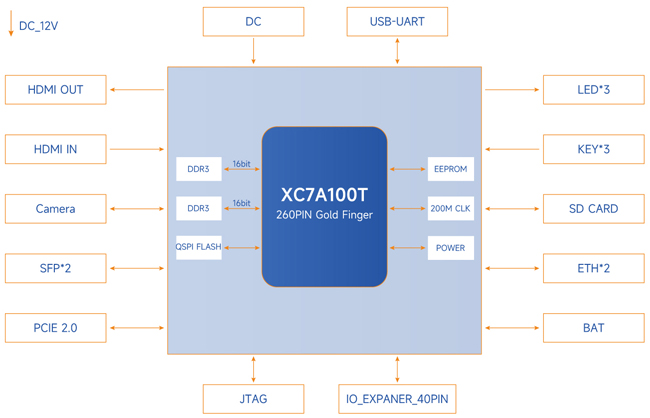
The MYD-J7A100T Development Board comprises the MYC-J7A100T System-On-Module (SOM) and a specially designed base board, which provides a fully equipped platform for evaluating and developing solutions based on AMD/Xilinx Artix-7 FPGAs. The MYD-J7A100T incorporates the XC7A100T (XC7A100T-2FGG484I) device from the Artix-7 series and extends a rich set of peripherals and interfaces on the base board through connectors and headers. These include two Gigabit Ethernet ports, two SFP+ interfaces, a PCIe 2.0 interface, HDMI input and output interfaces, a DVP camera interface, a Micro SD slot, a USB-UART interface, a FAN interface, and a 2.5mm pitch 2x 20-pin IO expansion interface.
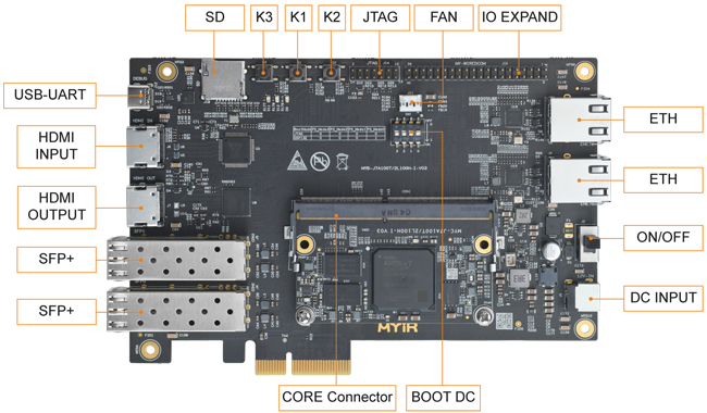
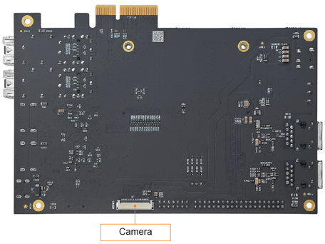
MYD-J7A100T Top-Bottom-view
- MYC-J7A100T SOM as Controller Board
- AMD/Xilinx XC7A100T Artix-7 FPGA (XC7A100T-2FGG484I)
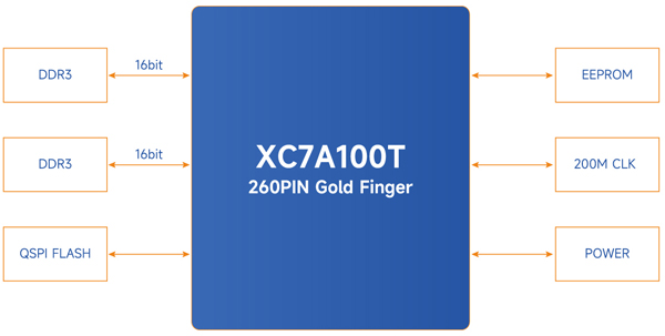
- 512MB DDR3, 32MB QSPI FLASH, 32KB EEPROM
- 2x Gigabit Ethernet, 2x SFP+, 1x PCIe, 1x USB-to-Uart, 1x Micro SD Card Slot, 1x JTAG
- HDMI Input and Output, DVP Camera Interface
- Optional RPI Module (RS232/RS485) and Camera Module
- Support Working Temperature Ranging from -40 to 85 Celsius
- Supports Development by Xilinx's Vivado Design Suite
The MYD-J7A100T board is capable of operating within industrial-grade temperatures, ranging from -40 to +85 Celsius, ensuring reliable performance in various environmental conditions. MYIR provides a range of Vivado sample codes for testing purposes, enabling users to quickly get started with developing their solutions.
The MYD-J7A100T Development Board comes with a Quick Start Guide, one USB Type-A to Type-C cable, and one 12V/2A power adapter. Additionally, MYIR offers optional accessories such as the MY-CAM011B Camera Module and the MY-WIREDCOM RPI Module (RS232/RS485), which can be integrated with the board to enhance its functionality and expand its application possibilities.
Features
Mechanical Parameters
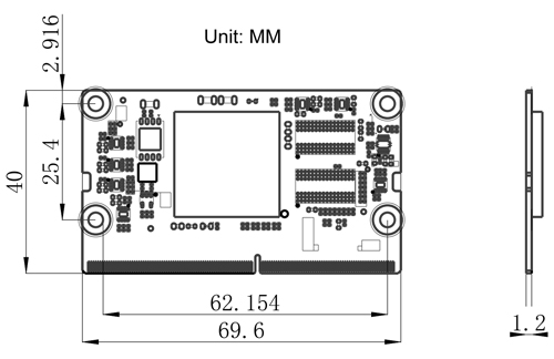
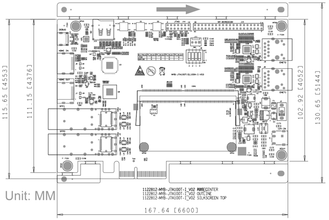
- Dimensions: 167.64mm x 130.65mm (base board), 69.6mm x 40mm (SOM)
- PCB Layers: 6-layer design (base board), 12-layer design (SOM)
- Power supply: 12V/2A (base board), 5V/3A (SOM)
- Working temperature: -40~85 Celsius
FPGA
- AMD/Xilinx XC7A100T Artix-7 FPGA (XC7A100T-2FGG484I)
Memory and Storage
- 512MB DDR3
- 32MB QSPI FLASH
- 32KB EEPROM
The MYD-J7A100T Development Board Base Board
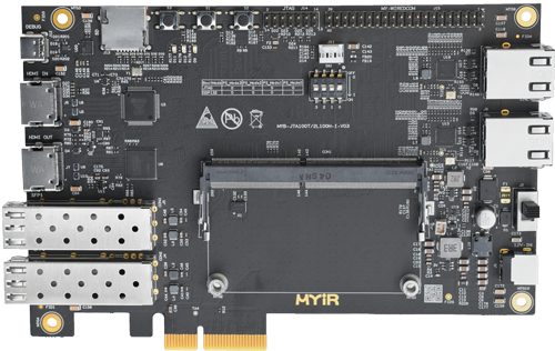
- 1 x Power jack
- 3 x Buttons
- 1 x Dip switch (for Boot selection and Power On/OFF)
- 1 x Micro SD card slot
- 1 x JTAG interface
- 2 x SFP+ interfaces
- 1 x PCIe 2.0 interface
- 2 x 10/100/1000 Mbps Ethernet interfaces
- 1 x USB-to-UART interface (Type C)
- HDMI input and output
- 1 x DVP digital camera interface
- Supports MYIR’s MY-CAM011B Camera Module
- 1 x 2.54mm pitch 40-pin male expansion header
- Supports MYIR’s MY-WIREDCOM RPI Module to extend RS232/RS485
Order Part No Packing List
| Item | Part No. | Packing List |
|---|---|---|
| MYD-J7A100T Development Board | MYD-J7A100T-32Q512D-I |
|
| MYC-J7A100T System-On-Module | MYC-J7A100T-32Q512D-I | One MYC-J7A100T Module |
Hardware Specification
The AMD/Xilinx Artix®-7 family of FPGAs has redefined cost-sensitive solutions by cutting power consumption in half from the previous generation while providing best-in-class transceivers and signal processing capabilities for high bandwidth applications. Built on the 28nm HPL process, these devices deliver best in class performance-per-watt. Together with the MicroBlaze(TM) soft processor, Artix-7 FPGAs are ideal for products like portable medical equipment, military radios, and compact wireless infrastructure. Artix-7 FPGAs meet the needs of size, weight, power, and cost (SWaP-C) sensitive markets like avionics and communications.
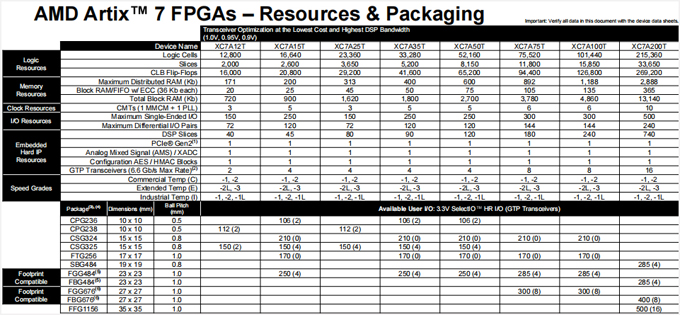
The MYC-J7A100T uses the XC7A100T-2FGG484I device, offering an extensive range of features including up to 101,440 logic cells, 4,860 Kb of Block RAM, 240 DSP slices, 929 GMAC/s, 8 GTP transceivers capable of reaching speeds up to 6.6Gb/s, x4 Gen2 PCIe interface, and a total of 285 I/O pins, all contained within the FGG484 package.
Software Features
MYIR provides a range of Vivado sample codes for testing purposes, enabling users to quickly get started with developing their solutions based on MYIR’s MYD-J7A100T development board. The provided project files are listed in below table:
| Vivado Project File | Description | Source Code |
|---|---|---|
| led_test | User LED Test | YES |
| key_test | Development Board Keys Test | YES |
| uart_test | UART Test | YES |
| hdmi_out_test | HDMI Output Interface Test | YES |
| ddr_test | DDR3 Test | YES |
| sd_hdmi_out | SD Card Read/Write Function Test | YES |
| hdmi_in_ddr_hdmi_out | HDMI Input Interface Test | YES |
| ov2659_ddr_hdmi_out | Camera Output Display Test | YES |
| sfp_test | SFP Loopback Test | YES |
| pcie_test | PCIe Read/Write Function Test | YES |
| udp_cmos_rgmii | Ethernet UDP Function Test | YES |
| İşlemci Tipi | : | TI |


