Terasic DE10-Standard Development Kit


Terasic DE10-Standard Development Kit
(P/N:P0493)
The DE10-Standard Development Kit presents a robust hardware design platform built around the Intel System-on-Chip (SoC) FPGA, which combines the latest dual-core Cortex-A9 embedded cores with industry-leading programmable logic for ultimate design flexibility. Users can now leverage the power of tremendous re-configurability paired with a high-performance, low-power processor system. Altera’s SoC integrates an ARM-based hard processor system (HPS) consisting of processor, peripherals and memory interfaces tied seamlessly with the FPGA fabric using a high-bandwidth interconnect backbone. The DE10-Standard development board includes hardware such as high-speed DDR3 memory, video and audio capabilities, Ethernet networking, and much more.
Board Comparisons
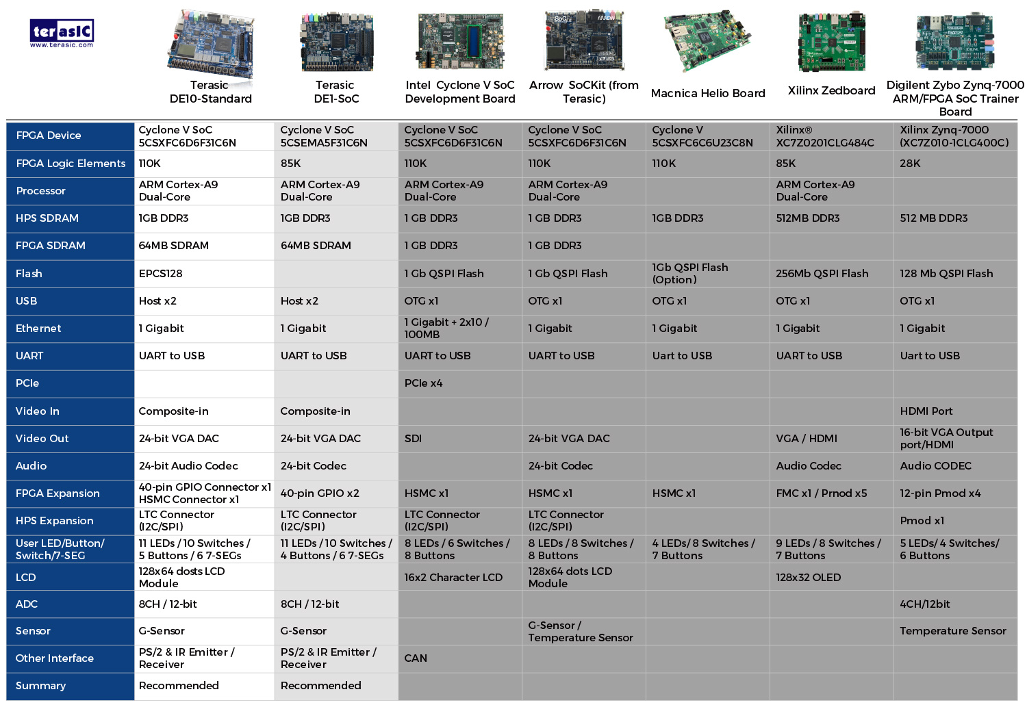
Specification
The DE10-Standard board has many features that allow users to implement a wide range of designed circuits, from simple circuits to various multimedia projects.
The following hardware is provided on the board:
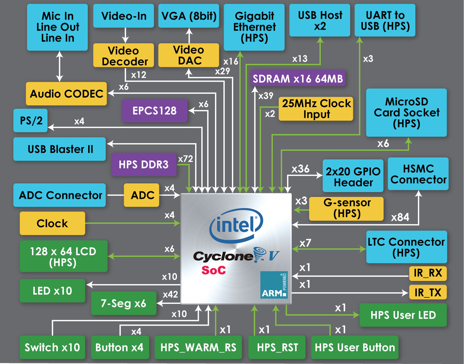
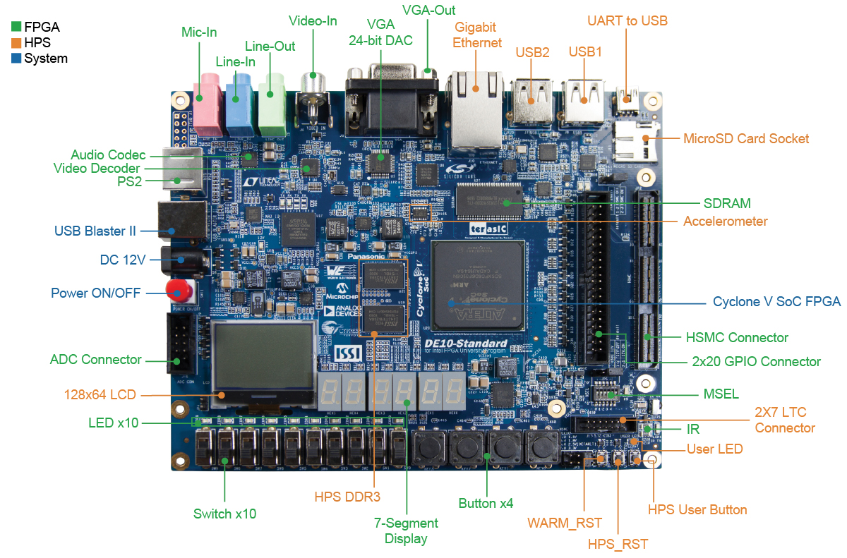
FPGA Device
- Cyclone V SX SoC—5CSXFC6D6F31C6N
- 110K LEs, 41509 ALMs
- 5,761 Kbits embedded memory
- 6 FPGA PLLs and 3 HPS PLLs
- 2 Hard Memory Controllers
ARM-Based Hard Processor System (HPS)
- 925 MHz, Dual-Core ARM Cortex-A9 MPCore Processor
- 512 KB of Shared L2 Cache
- 64 KB of Scratch RAM
- Multiport SDRAM Controller with Support for DDR2, DDR3, LPDDR1, and LPDDR2
- 8-Channel Direct Memory Access (DMA) Controller
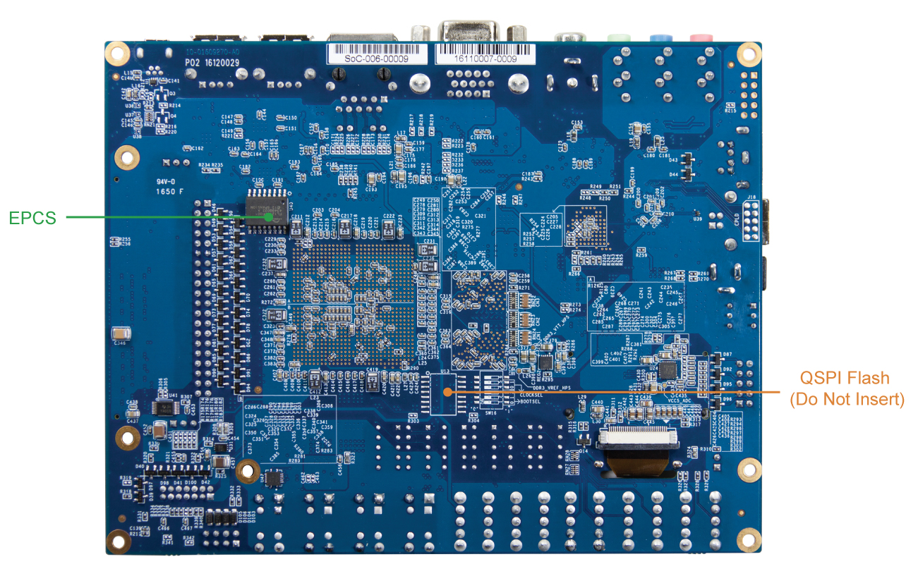
Configuration and Debug
- Serial Configuration Device – EPCS128 on FPGA
- On-Board USB Blaster II (Normal Type B USB Connector)
Memory Device
- 64MB (32Mx16) SDRAM on FPGA
- 1GB (2x256Mx16) DDR3 SDRAM on HPS
- MicroSD Card Socket on HPS
Communication
- Two USB 2.0 Host Ports (ULPI Interface with USB Type A Connector) on HPS
- USB to UART (Micro USB Type B Connector) on HPS
- 10/100/1000 Ethernet on HPS
- PS/2 Mouse/Keyboard
- IR Emitter/Receiver
Connectors
- One 40-pin Expansion Header (Voltage Levels: 3.3V)
- One HSMC Connector (Configurable I/O Standards 1.5/1.8/2.5/3.3V)
- One 10-Pin ADC Input Header
- One LTC Connector (SPI Master, I2C, and GPIO Interface) on HPS
Display
- 24-bit VGA DAC
- 128x64 Dots LCD Module with Backlight on HPS
Audio
- 24-bit CODEC, Line-in, Line-out, and Microphone-In Jacks
Video Input
- TV Decoder (NTSC/PAL/SECAM) and TV-In Connector
ADC
- Sample Rate: 500 KSPS
- Channel Number: 8
- Resolution: 12 bits
- Analog Input Range: 0 ~ 4.096 V
Switches, Buttons and Indicators
- 5 User Keys (FPGA x4, HPS x1)
- 10 User Switches (FPGA x10)
- 11 User LEDs (FPGA x10, HPS x1)
- 2 HPS Reset Buttons (HPS_RST_n and HPS_WARM_RST_n)
- 7-Segment Display x6
Sensors
- G-Sensor on HPS
Power
- 12V DC Input
Connectivity
- Connect LT24
- Connect MTL2
- Connect D8M
- Connect D5M
- Connect SMK
- Connect RFS
- Connect HTG
- Connect ADA
- Connect DCC
- Connect LTC2607 (AD/DA Daughter Card)
Block Diagram of the DE10-Standard Board
DE10-Standard Development Kit
DE10-Standard Development Kit
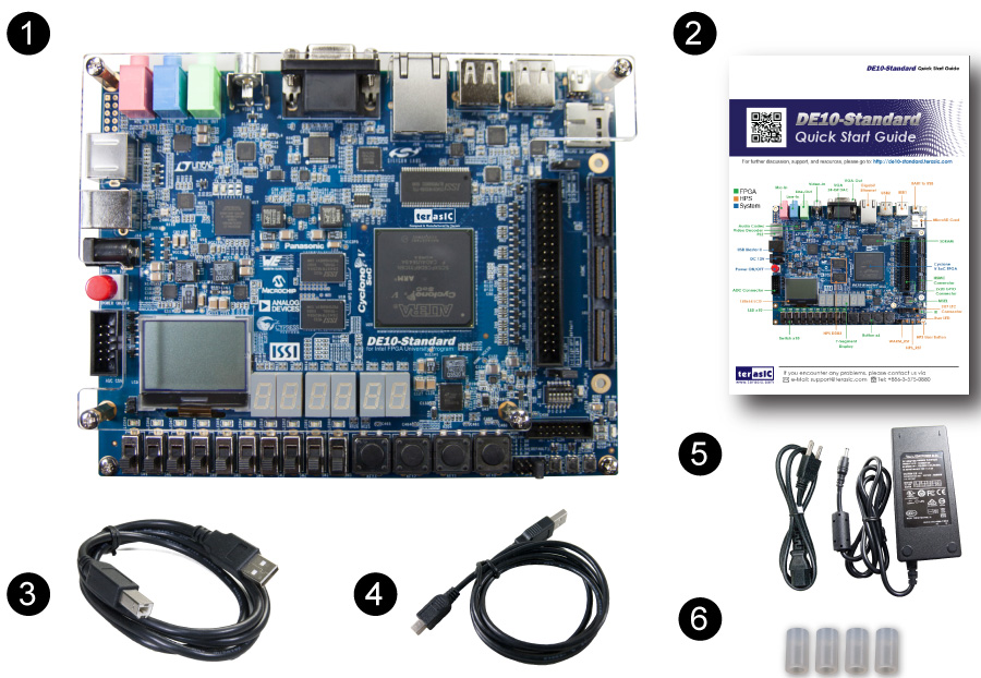
Package Include
- DE10-Standard Board
- DE10-Standard Quick Start Guide
- Type A to B USB Cable
- Type A to Mini-B USB Cable
- Power DC Adapter (12V)
- Four Silicon Footstands
Documents
CD-ROM
| Title | Version | Size | Date | Download |
|---|---|---|---|---|
| DE10-Standard CD-ROM | 1.3.1 | 2024-10-23 | ||
| DE10-Standard SystemBuilder | 1.0.1 | 2017-06-06 | ||
| Quartus Download | 16.1 | 2017-01-26 |
Daughter Card Demonstrations
| Title | Version | Size | Date | Download |
|---|---|---|---|---|
| HDMI-TX | 2018-12-21 | |||
| HDMI-RX | 2018-12-21 | |||
| D8M | 2018-01-26 | |||
| ADA | 2017-04-18 | |||
| D5M | 2017-04-18 | |||
| DCC | 2017-04-18 | |||
| LT24 | 2017-04-18 | |||
| MTL2 | 2017-04-18 | |||
| RFS | 2017-04-18 | |||
| SMK | 2017-04-18 |
Linux BSP (Board Support Package): MicroSD Card Image
BSP(Board Support Package) for Intel FPGA SDK OpenCL 16.1
BSP(Board Support Package) for Intel FPGA SDK OpenCL 18.0
More resources about IP and Dev. Kit are available on Intel User Forums.